

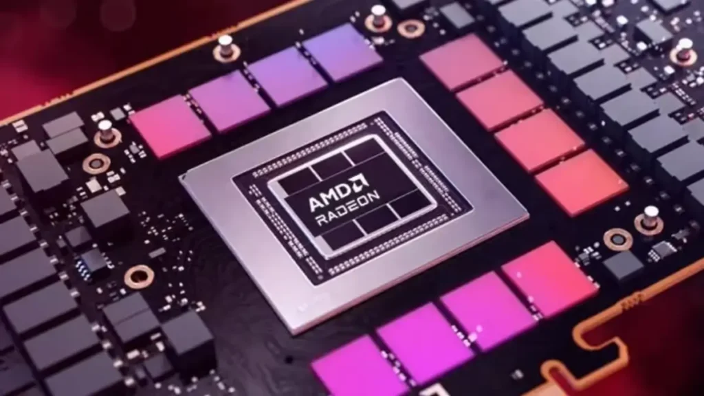
A wave of recently published AMD GPU patents offers one of the clearest looks yet at how the company plans to evolve real-time ray tracing and GPU scheduling. Rather than relying on larger chips or higher clock speeds, the filings describe smarter pipelines, more efficient geometry handling, and deeper hardware support for modern graphics APIs. These AMD GPU patents collectively reveal how the company is rethinking ray tracing hardware and GPU scheduling for the next generation of graphics processors.
Patents do not equal products. However, the technical focus across more than twenty related filings suggests AMD is preparing for a structural change in how future Radeon GPUs handle ray tracing workloads.
Background on AMD GPU Patents and Their Focus
AMD files hundreds of patents every year, but this particular group stands out for its cohesion. Out of 23 recently highlighted patents, fourteen target ray tracing performance, eight focus on GPU scheduling and execution, and one addresses on-chip data sorting. The overlap between these categories is important. Rather than treating ray tracing as a standalone feature, AMD appears to be redesigning the entire pipeline—from geometry storage to task scheduling—to reduce wasted computation.
Hardware Acceleration for Ray Traversal: The Missing Link
One of the most significant implications of the patents is a shift in how AMD handles ray tracing at the hardware level.
This gap is officially being closed with the introduction of Radiance Cores, a new dedicated hardware block confirmed for AMD’s upcoming UDNA (Unified DNA) architecture. While previous RDNA generations relied more heavily on software and general compute units for BVH traversal, Radiance Cores move this logic into dedicated silicon. This effectively grants AMD feature parity with NVIDIA’s RT cores, allowing the GPU to handle the entire ray tracing search process without taxing general compute resources.
Several of the recent AMD GPU patents describe the technical groundwork for this transition. They outline hardware methods for accelerating BVH traversal, smarter node tagging to skip irrelevant geometry, and low-precision filtering to reject rays early in the pipeline. Taken together, these filings map directly to the kind of functionality required for Radiance Cores to operate efficiently in real-time gaming workloads.
AMD GPU Patents and Dense Geometry Format Acceleration
Another major theme across the patents is AMD’s work on Dense Geometry Format (DGF), which has already existed as a software feature within the GPUOpen SDK.
AMD has now transitioned DGF from a software-only capability to a hardware-accelerated standard known as Universal Compression. By integrating a fixed-function decompression engine directly into the shader engines, future GPUs can handle “Nanite-level” geometric detail with significantly lower performance overhead. This shift ensures that the massive data sets required for modern path tracing do not overwhelm GPU memory bandwidth.
In practical terms, this means that future Radeon architectures will be able to process extremely complex scenes without the dramatic slowdowns that traditionally accompany high-polygon ray-traced environments.
Physics and Visual BVHs: A Practical Reality Check
One patent proposes a unified BVH structure for both ray tracing and physics collision detection. To address the discrepancy between high-detail visual meshes and simplified physics proxies, AMD appears to be utilizing a Multi-Resolution BVH. This allows the hardware to query the same data structure at different levels of detail—saving memory by storing one “map” of the world that serves both the renderer and the physics engine.
If implemented as described, this approach could streamline game development pipelines while reducing duplicated data and improving overall performance efficiency.
Work Graphs Scheduling: Aligning Hardware with Industry Standards
Not all of the patents are about ray tracing alone. A significant group centers on advanced scheduling systems based on Microsoft’s Work Graphs API, a core part of the modern DirectX 12 Agility SDK.
These filings propose methods for shader engines to schedule and dispatch their own workloads autonomously, improving load balancing across GPU cores. They also describe communication systems that allow GPUs to manage large numbers of small tasks more effectively and scale efficiently to very wide or chiplet-based GPU designs.
Because Work Graphs are becoming an industry standard, these patents could benefit not only future games but also professional applications that rely on complex GPU computation. The involvement of Matthäus Chajdas, one of the architects of the Work Graphs API, as an inventor on several filings strongly indicates that AMD’s research is aligned with real, shipping software ecosystems.
Separating Facts From Speculation
Several facts are clearly established. The patents themselves are real and publicly available, and they explicitly describe AMD research into hardware acceleration for BVH traversal. Dense Geometry Format is already a shipping software feature, and Microsoft Work Graphs is a confirmed industry API rather than experimental technology. The filings also show that AMD is working on both ray tracing performance and next-generation GPU scheduling at the same time.
What remains speculative is how and when these ideas will reach real products. It is not yet known which GPU generations will include these features, whether they will first appear in consumer Radeon cards or console hardware, or what exact performance gains they might deliver in practice. Given AMD’s role as the silicon provider for PlayStation and Xbox hardware, it is reasonable to assume that some of these ideas could influence next-generation consoles, but no official confirmation exists.
Implications of AMD GPU Patents for Future Radeon GPUs
If these patents translate into real hardware, they would represent a meaningful architectural shift. AMD would be moving ray traversal into dedicated hardware, reducing memory traffic through Dense Geometry Format acceleration, enabling smarter API-driven scheduling at the silicon level, and laying the groundwork for more scalable chiplet-style GPU designs.
Rather than matching NVIDIA feature-for-feature, AMD appears to be building a pipeline optimized for efficiency and data locality. This mirrors the philosophy that made AMD’s Zen CPU architecture successful: do more with the same resources by eliminating bottlenecks.
Comparison of AMD Ray Tracing Patents With Competing Approaches
Today, NVIDIA generally holds the performance lead in ray tracing thanks to years of investment in dedicated RT cores and software ecosystems. AMD’s existing GPUs support ray tracing, but they typically rely more on general-purpose compute resources.
The techniques outlined in these patents suggest AMD may be aiming for a different path. Instead of copying NVIDIA’s model, the company seems to be designing systems that streamline the entire ray tracing process, from geometry storage to workload scheduling. If successful, this could allow AMD to close the performance gap without needing dramatically larger or more expensive chips.
Expert Analysis: A Coherent Strategy, Not Isolated Ideas
Taken as a whole, the filings suggest AMD is pursuing a coordinated redesign of its ray tracing pipeline rather than isolated experiments. The ideas revolve around reducing data movement, avoiding unnecessary calculations, and dynamically balancing workloads across GPU cores. By sharing structures between ray tracing and physics, filtering out unnecessary rays early, and making scheduling more intelligent, AMD could improve performance without simply increasing transistor counts.
The mention of chiplet-friendly GPU designs is particularly noteworthy. AMD already revolutionized CPUs with modular Zen architectures, and similar concepts applied to GPUs could lead to highly scalable designs in the future.
What We Still Don’t Know
Despite the detailed nature of the patents, many questions remain. It is unclear which of these techniques AMD plans to prioritize, or how soon any of them might appear in consumer products. Patents can represent long-term research that takes years to become reality. Until AMD announces new hardware, these filings should be viewed as hints rather than promises.
All in all the latest AMD GPU patents provide a fascinating look at how the company is preparing for the next era of graphics technology. Rather than chasing raw power alone, AMD seems focused on building smarter, more efficient systems for ray tracing and workload management.
Whether these ideas debut in upcoming Radeon GPUs or next-generation consoles remains to be seen. For now, they offer an intriguing preview of where AMD graphics innovation may be headed.
FAQ
What do these AMD GPU patents reveal?
They show AMD researching hardware acceleration for ray traversal, better BVH handling, and deeper integration with Microsoft Work Graphs scheduling.
Does AMD already have ray tracing hardware?
Yes. Current GPUs accelerate intersection tests, but traversal is mostly done in general compute—something these patents aim to change.
Is Dense Geometry Format new?
No. DGF is already a software feature. The patents describe adding dedicated hardware support for it.
Are Work Graphs speculative technology?
No. Work Graphs is an existing DirectX standard, and AMD is aligning future hardware with it.
Could this technology appear in future consoles?
Possibly, since AMD designs custom chips for PlayStation and Xbox, but there is no official confirmation.
More News
GTA 6 Leaks: Story, Gameplay & Map Rumors Explained
No Resident Evil 5 Remake Announcement This Year as Code Veronica Remake Is Scheduled Next
Rockstar Bans GTA Online Missions Recreating Charlie Kirk Assassination