


TSMC’s upcoming A14 manufacturing process is reportedly set to deliver its first significant SRAM cell-size reduction in eight years, potentially allowing future CPUs and GPUs to accommodate more cache memory within the same silicon area. The company’s high-density six-transistor (6T) SRAM bitcell is expected to shrink below 0.017 square micrometers (µm²), compared with approximately 0.021 µm² used since its N5 process debuted in 2020.
The development was detailed on October 26 by South Korean semiconductor publication ETNews, which reported that TSMC has achieved the smaller cell size and plans to present its research findings later this year. The reported measurement represents a reduction of more than 19% in individual SRAM cell area, addressing a scaling limitation that has persisted across several generations of advanced semiconductor manufacturing.
SRAM, or static random-access memory, provides the high-speed storage used in processor caches. Unlike conventional system RAM, SRAM is integrated directly into processors, allowing CPU and GPU cores to access frequently needed data without repeatedly retrieving it from slower external memory.

While manufacturers have continued shrinking logic transistors to improve processor density, SRAM cells have proven considerably harder to reduce. These cells must maintain reliable data storage and read/write operations, creating design constraints that become increasingly difficult to manage at smaller dimensions.
TSMC’s high-density 6T SRAM cells have remained around 0.021 µm² since the company’s 5nm-class N5 process. Subsequent manufacturing generations, including N3 and N2, have not delivered comparable improvements in SRAM cell area, even as their logic transistor technologies advanced.
The reported A14 development could change that balance. Reducing individual bitcell area below 0.017 µm² would increase theoretical raw cell density by more than 23% compared with the previous 0.021 µm² design, although actual cache density improvements would also depend on supporting circuitry and memory-array layouts.
For PC processor manufacturers, smaller SRAM cells could provide greater flexibility when designing cache-heavy CPUs and GPUs. Engineers could potentially increase cache capacity without proportionally increasing silicon area or retain existing cache configurations while allocating more chip space to other components.
Larger on-chip caches can reduce the frequency of accesses to external memory, which may benefit workloads sensitive to memory latency and bandwidth. However, the reported SRAM improvement does not establish any specific gaming-performance increase. Actual results would depend on processor architecture, cache configuration, operating frequencies and software workloads.
ETNews also reported that TSMC’s A14 SRAM cell would be smaller than the 0.021 µm² high-density cell disclosed for Intel’s 18A process. Direct comparisons with Samsung’s latest manufacturing technologies remain difficult because equivalent SRAM cell measurements have not been publicly established.
The smaller SRAM design is separate from TSMC’s previously announced improvements to its A14 manufacturing process.
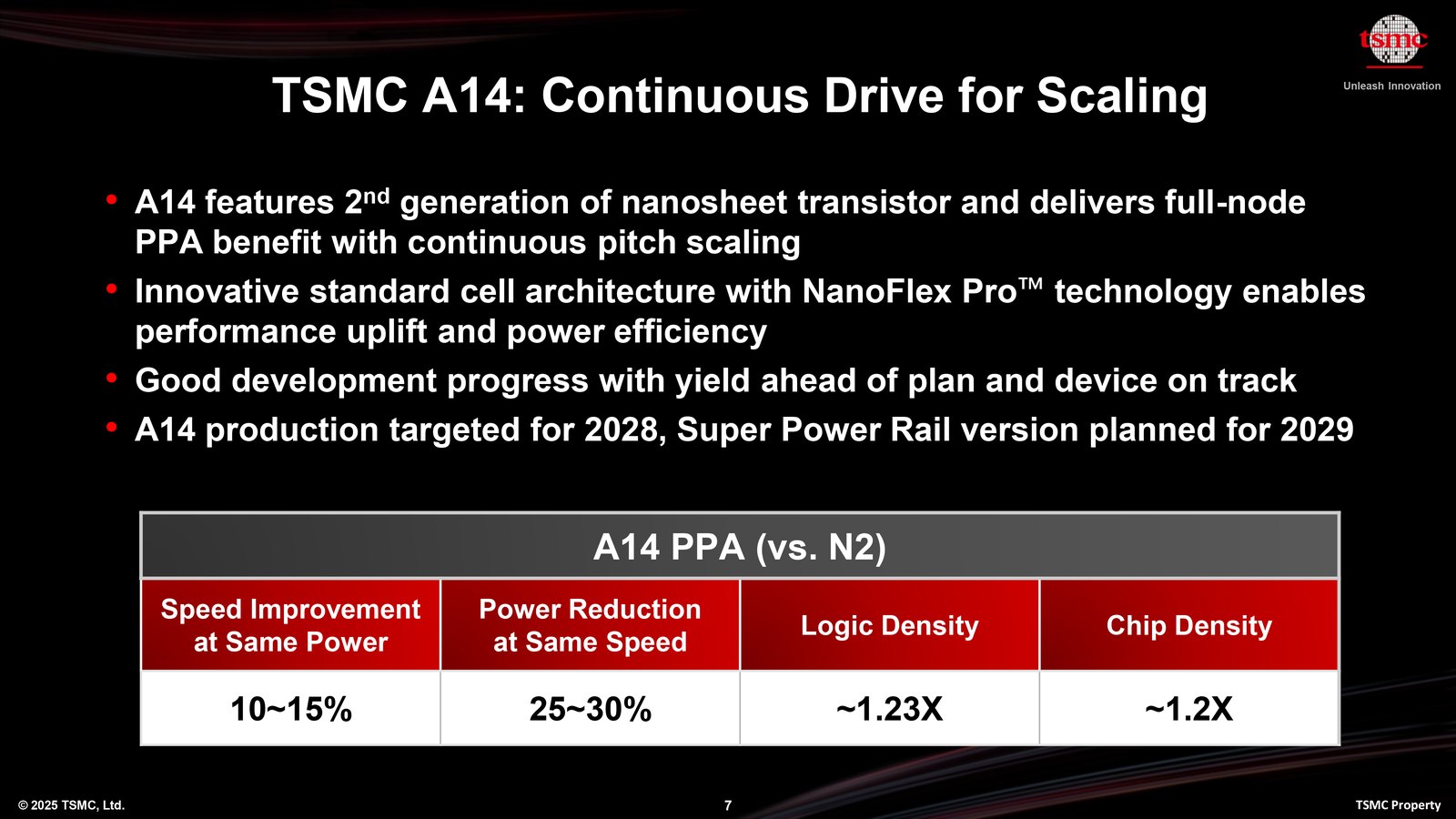
According to the company’s official technology roadmap, A14 is designed to deliver a 10–15% performance improvement at the same power consumption or a 25–30% reduction in power consumption at the same performance level compared with N2. TSMC also expects approximately 20% higher overall chip density.
These figures represent alternative process-level performance and efficiency targets rather than guaranteed improvements for finished consumer processors.
TSMC previously confirmed that A14 development was progressing on schedule. During its July 2026 earnings presentation, the company disclosed that an internal test vehicle had demonstrated approximately 90% of targeted device performance and close to 90% yield for a 256Mb SRAM test structure.
The company also reported customer engagement across smartphone and high-performance computing applications, with risk production scheduled for 2027 and volume manufacturing planned for 2028.
However, TSMC has not publicly provided detailed commercial specifications for the newly reported sub-0.017 µm² SRAM design. Its final production yield, manufacturing costs and adoption by individual chip designers remain unconfirmed.
The development is also distinct from the broader memory supply constraints expected to persist through 2028. SRAM is fabricated within processors rather than supplied as separate DRAM or HBM memory chips, meaning improved SRAM scaling would not directly resolve shortages in those markets.
TSMC’s reported advancement could give future processor designers another way to increase on-chip cache capacity as logic transistor scaling continues. Whether the technology ultimately benefits gaming CPUs and GPUs will depend on which manufacturers adopt A14 and how they incorporate its improved SRAM density into commercial products.
